Any channel noise output (without high-pass filter)
Channel 1 noise output (with high-pass filter)
Channel 2 noise output (with high-pass filter)
Noise filter
There are four semi-independent audio channels, each with its own frequency, noise and volume control. Each channel has an eight-bit "divide-by-N" frequency divider and an eight-bit control register, which selects the noise (polynomial counter) content and volume.
There are six key scan line (K0-K5), which holds a value from 00 to 3F. There are two sense lines. One of the sense lines is for the full decode of the six scan lines. The other sense line is for decoding only the codes (CTRL, SHIFT and BREAK key).
There are eight pot ports for measuring input rise time. Each input has an eight-bit counter which is clocked every TV line. Each input also has a dump transistor which is turned on or off by software.
There are three timer which use the audio channels. If start timer (STIMER) is enabled, the audio channels are reset.
There is a Random Number Generator which is eight bits from a polynomial counter.
There is a serial I/O port. The serial port consists of a serial output line, a serial input line, a serial output clock line, and a bi-directional serial data clock line. Also, there are control register which are used to configure the serial port.
There are eight IRQ interrupt. They are BREAK key, OTHER key, SERIAL INPUT READY, SERIAL OUTPUT NEEDED, TRANSMISSION FINISHED, TIMER #4, TIMER #2 and TIMER #1. These interrupts can be enabled or disabled by software. There is also a register to read interrupt status.
There are four semi-independent audio channels, each with its own frequency, noise and volume control. Each channel has an eight-bit "divide-by-N" frequency divider and an eight-bit control register (AUDFX). Each channel also has an eight-bit control register (AUDCX) which selects the noise (polynomial counter) content and the volume.
All four frequency dividers can be clocked simultaneously from 64 kHz or 15 kHz by AUDCTL bit 0. Frequency dividers 1 and 3 can alternately be clocked from the CPU clock (1.79 MHz NTSC, 1.77 MHz PAL) by setting AUDCTL bits 5 and 6. Frequency dividers 2 and 4 can alternately be clocked with the output of dividers 1 and 3 by setting AUDCTL bits 4 and 3. This allows the following options: 4 channels of 8-bit resolution, 2 channels of 16-bit resolution, or 1 channel of 16-bit resolution and 2 channels of 8-bit resolution.
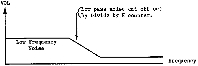
There are three polynomial counters (17 bit, 5 bit and 4-bit) used to generate randowm noise. The 17-bit poly counter can be reduced to a 9-bit poly counter by bit 7 of AUDCTL. These counters are clocked byt 1.79 MHz. Their outputs, however, can be sampled independently by the four audio channels at a rate determined by each channel's frequency divider. Thus each channle appears to contain seperate poly counters clocked at its own frequency. This oly counter noise sampling is controlled by bits 5, 6 and 7 of each AUDCX register. Because the poly counters are sampled by the "divide-by-N" frequency divider, the output obviously cannot change faster than the sampling rate. In these modes (poly noise outputted), the dividers are therefore acting as "low-pass" filter clocks, allowing only the low-frequency noise to pass.
The output of the noise-control circuit described above consists of pure tones (square wave type), or polynomial counter noise at a maximum frequency set by the "divide-by-N" counter (low pass clock). This output can be routed through a high-pass filter if desired by use of bits 1 and 2 of AUDCTL.
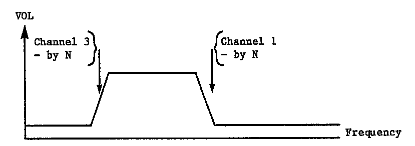
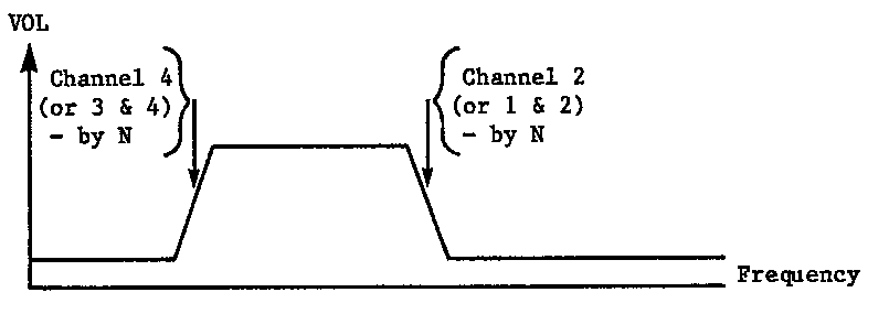
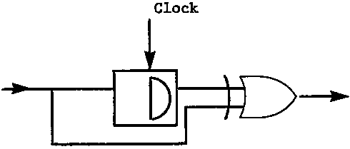
The high-pass filter consists of a D-type flip-flop and an exclusive-OR gate. The noise control circuit output is sampled by this flip flop at a rate set by the "high-pass" clock. The input and output of the flip-flop pass through the exclusive-OR gate. However, if it is lower than the clock rate, the flip-flop output will tend to follow the input and the two exclusive-OR gate inputs will mostly be identical (11 or 00) givving very littl output. This gives the effect of a crude high-pass filter, passing only noise whose minimum frequency is set by the high-pass clock rate. Only channels 1 and 2 have such a high-pass filter. The high-pass clock for channel 1 comes from the channel 3 divider. The high-pass clock for channel 2 comes from the channel 4 divider. This filter is only included if bit 1 or 2 of AUDCTL is true.
A volume control ciruit is placed at the output of each channel. This is a crude 4-bit digital to analog converter that allows sellection of one of 16 possible output current levels for a true audio input. A logic zero audio input to this voulme circuit always gives an open-circuit (zero current) output. The volume selection is controlled by bits 0 through 3 of AUDCX. "Volume Control only" mode can be invoked by forcing this circuit's audio input true with bit 4 of AUDCX. In this mode the dividers, noise counters, and filter circuits are all disconnected from the channel output. Only the volume control bits (0 to 3 of AUDCX) determine the channel output current.
The audio output of any channel can be completely turned off by writing zero to the volume control bits of AUDCX. All ones give maximum volume.
Any channel noise output (without high-pass filter)
Channel 1 noise output (with high-pass filter)
Channel 2 noise output (with high-pass filter)
Noise filter
This address writes data into the Audio Mode Control Register (also see SKCTL two-tone bit 3 and notes).
7 6 5 4 3 2 1 0 if set, this bit: 1 change normal clock base from 64 kHz to 15 kHz 1 inserts high-pass filter into channel 2, clocked by chan 4 1 inserts high-pass filter into channel 1, clocked by chan 3 (see section 2) 1 clock channel 4 with channel 3, instead of 64 kHz (16-bit) 1 clock channel 2 with channel 1, instead of 64 kHz (16-bit) 1 clocks channel 3 with 1.79 MHz, instead of 64 kHz 1 clocks channel 1 with 1.79 MHz, instead of 64 kHz 1 makes the 17-bit poly counter into a 9-bit poly counter.
Exact Frequencies
The frequencies given above are approximate. The exact frequency (Fin) that clocks the divide-by-N counters is given below (NTSC only, PAL is different).
Fin Approx Exact (NTSC) Exact (PAL) 1.79 MHz 1.78979 MHz Use modified formula for Fout 64 kHz 63.9210 kHz 15 kHz 15.6999 kHz Use normal formula for Fout
The Normal formula for the output frequency is:
Fout = Fin /2N
where N = the binary number in the frequency register (AUDF), plus 1 (N=AUDF+1).
The Modified formula should be used when Fin = 1.79 MHz and a more exactl result is desired:
Fout = Fin /2(AUDF+M)
where
M = 4 if 8 bit counter (AUDCTL bit 3 or 4 = 0),
M = 7 if 16 bit counter (AUDCTL bit 3 or 4 = 1)
These addresses write data into each of the four Audio Frequency Control Registers. Each register controls a divide-by-N counter.
D7 D6 D5 D4 D3 D2 D1 D0 "N" 00000000 1 00000001 2 etc. 11111111 256
Note "N" is 1 greater than the value in Audio Frequency Register AUDF(X).
These addresses write data into each of the four Audio Control Registers. Each register controls the noise content and volume of the corresponding Audio Channel.
Noise Content or Distortion, and Volume
D7 D6 D5 D4 D3 D2 D1 D0 HEX volume: 0 0 0 0 0 Lowest Volume (Off) 8 1 0 0 0 Half Volume etc F 1 1 1 1 Highest Volume Distortion:
Divisor "N" set by audio frequency register.0 0 0 0 0 17 Bit poly - 5 Bit poly - N 2 0 0 1 0 5 Bit poly - N - 2 4 0 1 0 0 4 Bit poly - 5 Bit poly - N 6 0 1 1 0 5 Bit poly - N - 2 8 1 0 0 0 17 Bit poly - N A 1 0 1 0 Pure Tone - N - 2 C 1 1 0 0 4 Bit poly - N 1 X X X 1 Force Output Volume only
PITCH VALUES FOR THE MUSICAL NOTES - AUDCTL=0, AUDC = hex AX
| AUDF | |||
| Hex | Dec | ||
| HIGH NOTES | C | 1D | 29 |
| B | 1F | 31 | |
| A# or Bb | 21 | 33 | |
| A | 23 | 35 | |
| G# or Ab | 25 | 37 | |
| G | 28 | 40 | |
| F# or Gb | 2A | 42 | |
| F | 2D | 45 | |
| E | 2F | 47 | |
| D# or Eb | 32 | 50 | |
| D | 35 | 53 | |
| C# or Db | 39 | 57 | |
| C | 3C | 60 | |
| B | 40 | 64 | |
| A# or Bb | 44 | 68 | |
| A | 48 | 72 | |
| G# or Ab | 4C | 76 | |
| G | 51 | 81 | |
| F# or Gb | 55 | 85 | |
| F | 5B | 91 | |
| E | 60 | 96 | |
| D# or Eb | 66 | 102 | |
| D | 6C | 108 | |
| C# or Db | 72 | 114 | |
| MIDDLE C | C | 79 | 121 |
| LOW NOTES | B | 80 | 128 |
| A# or Bb | 88 | 136 | |
| A | 90 | 144 | |
| G# or Ab | 99 | 153 | |
| G | A2 | 162 | |
| F# or Gb | AD | 173 | |
| F | B6 | 182 | |
| E | C1 | 193 | |
| D# or Eb | CC | 204 | |
| D | D9 | 217 | |
| C# or Db | E6 | 230 | |
| C | F3 | 243 | |
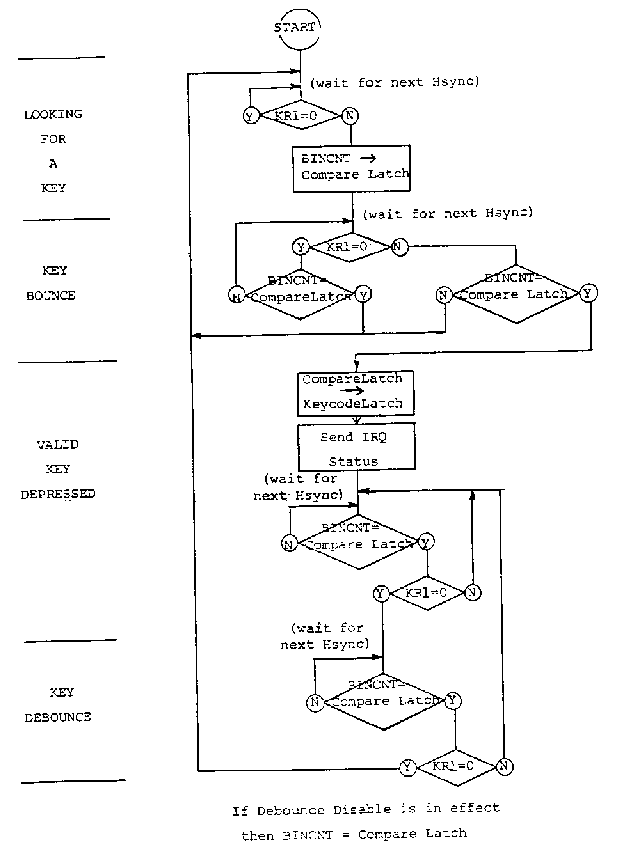
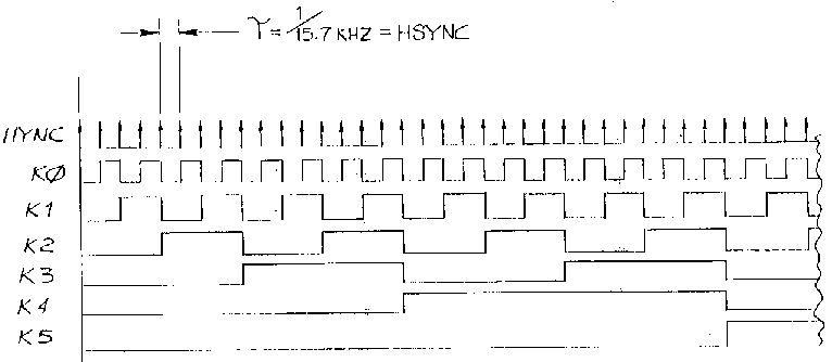
The !K0-!K5 lines hold a 6-bit value from 00 to 3F. This allows for decoding 64 keys. With externnal CMOS (4052) chips, a key matrix is formed. The value of the key selected by the matrix is returned on the !KR1 line.
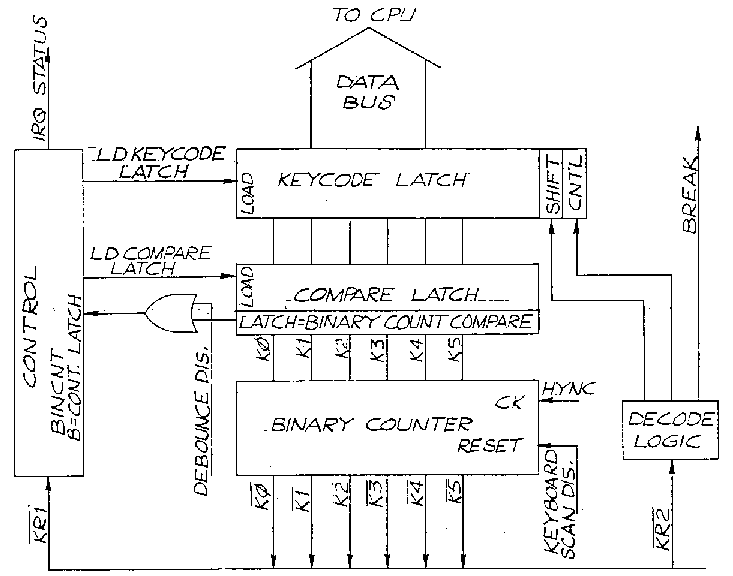
Inside the POKEY is a 6-bit binary counter, a 6-bit compare latch, and an 8-bit key code latch. A control state machine does the debouncing of the keys.
When the keyboard scanner is enabled by the SKTL register, the binary counter begins to count, once per line. If the !KR1 line goes low, the value of the binary counter is transferred to the compare latch. This will be the key code to be debounced. If !KR1 goes low before the next time the binary counter equals the compare latch the there are two keys depressed and both are ignored. If the binary counter equals the compare latch and !KR1 is high, then the key is bouncing and is ignored, but if !KR1 is low then the key is valid and it is transferrred to the keycode latch for reading by the CPU. An IRQ is also sent indicating the key is ready. As soon as !KR1 is low and the binary counter equals the compare latch and !KR1 is high, then the key is debounced and another key can be looked for. But if !KR1 is low, then the key is bouncing and is assumed to be still pressed.
If the debounce is disabled, the POKEY forces the binary counter equal compare latch signal to a logic true value which will disable debounce.
!KR2 input is used to decode 3 keys. They are SHIFT, BREAK and CONTROL. They do not get debounced. They are only decoded at:
| !K0 | !K1 | !K2 | !K3 | !K4 | !K5 | |
| 1 | 1 | 1 | 1 | 0 | 0 | = BREAK |
| 1 | 1 | 1 | 1 | 0 | 1 | = SHIFT |
| 1 | 1 | 1 | 1 | 1 | 1 | = CONTROL |
KBCODE (Keyboard Code)(09)
This address reads the Keyboard Code, and is usually read in response to a Keyboard Interrupt (IRQ and bits 6 or 7 of IRQST). See IRQEN for information on enabling keyboard interrupts. See SKCTL bits 1 and 0 for key scan and debounce enable.
D7 D6 D5 D4 D3 D2 D1 D0 Key code Shift Key Control Key
Read by OS into shadow CH when key is hit. The OS has a get character function which converts the keycode to ATASCII (Atari ASCII).
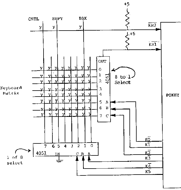
| !K0 | !K1 | !K2 | !K3 | !K4 | !K5 | |
| CNTL | 1 | 1 | 1 | 1 | 1 | 1 |
| SHIFT | 1 | 1 | 1 | 1 | 0 | 1 |
| BRK | 1 | 1 | 1 | 1 | 0 | 0 |
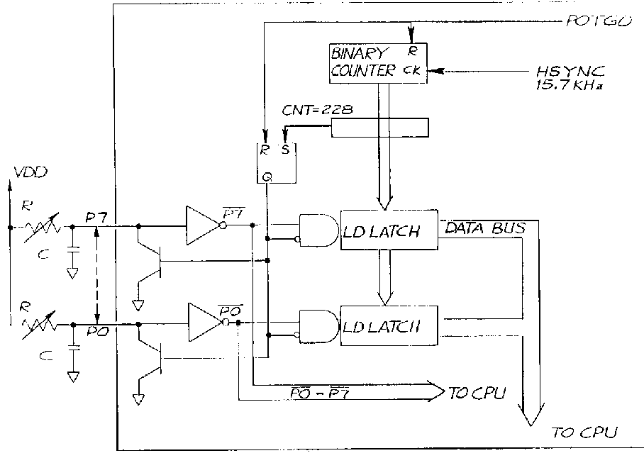
There are eight pot input lines. Each line has a dump transistor and an egiht-bit latch. There is a binary counter that will count to 228. The counter is reset by strobing POTGO, which also releases the dump transistors. It also starts the binary counter to count once per line. The pot lines will now start to charge. When each line reaches a logic on, it will cause the counter value to be latched into its corresponding latch to be read by the CPU. When the counter reaches 228, the dump transistor is turned on to pull the pot lines back to ground. The value in the latches will remain until the next POTGO strobe. To operate the pot port:
- Read POT0 to POT7 registers
- Write to POTGO register (strobe)
There is an ALLPOT register which allos the logic value of each pot line to be read by the CPU. The main use of Allpot is in the fast scan mode. This is done by:
NOTE: This address (as well as the fast scan mode) is useful only when the charging capacitors on the P0-P7 pads are removed, unless the pads are driven by buffer drivers.
POT0- POT7 (Pot values)(00-07):
These addresses read the value (0 to 228) of 8 pots (paddle controllers) connected to the 8-line pot port. The paddle controllers are numbered from left to right when facing the console keyboard. Turning the paddle knob clockwise results in decreasing pot values. The values are only valid after 228 TV lines following the POTGO command described below or after ALLPOT changes.
| D7 | D6 | D5 | D4 | D3 | D2 | D1 | D0 | Each pot value (0-228) |
ALLPOT (All Pot Lines Simultaneously)(08):
This address reads the present digital value of the eight-lin pot port.
| D7 | D6 | D5 | D4 | D3 | D2 | D1 | D0 | |
| P7 | P6 | P5 | P4 | P3 | P2 | P1 | P0 | Eight Pot Line States |
0 = Pot line register value is valid
1 = Pot line register value is not valid
POTGO (Start Pot Scan) (0B):
| D7 | D6 | D5 | D4 | D3 | D2 | D1 | D0 | No data bits used |
This write address starts the pot scan sequence. The pot values (POT0 - POT7) should be read first. This write strobe is then used causing the following sequence:
Three of the audio channels can be used as timers. Audio channles 1, 2 and 4 are the channels that will cause IRQ interrupts or the timers. If interrupts are enabled, the interrupts will be caused by the audio channel crossing zero. The audio channel divide can be set to their "AUDF" value by strobing the STIMER register. By Strobing STIMER, the audio outputs are forced to a known state which are logic high for channels 1 and 2, and logic low for channels 3 and 4.
STIMER (Start Timer) (09):
| D7 | D6 | D5 | D4 | D3 | D2 | D1 | D0 | No data bits used |
There is a seventeen bit polynomial counter that the CPU can read eight bits from. The polynomial counter can be changed to nine bits by use of AUDCTL. If the POKEY is in the initial state (see SKTLS), the counter is set to all ones state, therefore the CPU will read $FF.
RANDOM (Random Number Generator) (0A):
This address reads the high-order eight bits of a polynomial counter (nine bits if bit 7 of AUDCTL = 1).
| D7 | D6 | D5 | D4 | D3 | D2 | D1 | D0 |
The serial port consists of a serial data output (transmission) line, a serial data input (receiver) line, a serial output clock line, a bi-directional serial data clock line, and othe miscellaneous control lines described in the Operating System Manual.
Data are transmitted and received as 8 bits of serial data preceded by a logic zero start bit, and succeeded by a logic true stop bit. Input and output clocks are equal to the baud rate, not 16 times the baud rate. Transmitted data change when the output clock goes true. Received data is sampled when the input clock goes to zero.
Serial Output
The transmission sequence begins when the processor writes a byte to the serial output register (SEROUT). When any previous data byte transmission is finished the hardware will automatically transfer new data (from SEROUT) to the output shift register, interrupt the procesor to indicate an empty SEROUT register (ready to be reloaded with the next byte of data), and automatically serially transmit the shift register contents with start-stop bits attached. If the processor responds to the interrupt, and reloads SEROUT before the shift register is completely transmitted, the serial transmission will be smooth and continuous.
Output data is normally transmitted aslogic levels (+4V = true, 0V = false). Data can also be transmitted as two-tone information. This mode is selected by bit 3 of SKCTL. In this mode audio channel 1 is transmitted in place of logic true, and audio channel 2 is transmitted in place of logic false. Channel 2 must be the lower tone of the tone pair.
The processor can force the data output line to zero (or to audio channel 2, if in two-tone mode) by setting bit 7 of SKCTL. This is required to force a break (ten zeros) code transmission.
Serial Output Clock
The serial output data always changes when the serial output clock goes true. The clock the returns to zero in the center of the output data bit time.
The baud (bit) rate of the data and clock is determined by audio channel 4, audio channel 2, or by the input clock, depending on the serial mode selected by bits 4, 5, and 6 of SKCTL. See chart at end of this section.
Serial Input
The receiving sequence begins when the hardware has received a complete 8-bit serial data word plus start and stop bits. This data byte is automatically transfered to the 8-bit parallel input register (SERIN), and the processor is interrupted to indicate an input data byte is ready to be read from SERIN. The processor must respond to this interrupt, and read SERIN, before the next input data word eception is complete, otherwise an input data "over-run" will occur. Theis over-run will be indicated by bit 5 of SKSTAT (if bit 5 of IRQST is not reset (true) before the next input is complete), and means input data have been lost. This bit should be tested whenever SERIN is read. Bit 7 of SKSTAT should also be tested to detect frame erors caused by extra (or missing) data bits.
Direct Serial Input
The serial data input line can be read directly by the processor if desired, ignoring the shift register by reading bit 4 of SKSTAT.
Bi-directional Clock
This clock line is used to either receive a clock from an external clock source for clocking transmitted or received data, or is used to supply a clock to external devices indicating transmit or reception rate. This clock line direction is determined by the serial mode selected by bits 4, 5 and 6 of SKCTL (see mode chart at end of this section). Transmitted data changes on the rising edge of this clock. Received data is sampled on the trailing edge of this clock.
Asynchronous Serial Input
Unclocked serial data (at an approximately known rate ±5%) can be recieved in the asynchronous modes. The receive (input) shift register is clocked by audio channel 4. Channels 3 and 4 should be used together (AUDCTL bit 3 = 1) for increased resolution. In asynchronous modes, channels 3 and 4 are reset bye each start bit at the beginning of eah serial data byte. This allows the serial data rate to be slightly diferent from the rate set by channels 3 and 4.
Serial Mode Control
There are six useful modes (of the possible eight) controlled by bits 4, 5 and 6 of SKCTL. These are described on the next page.
Note that the two-tone output (bit 3 of SKCTL) may be used in any of these mdes except for the bottom pair. This is because channel 2 is used to set the output transmit rate and is therefore not available for one of the two tones.
Note that the output clock rate is identical to the output data rate.
SKSTAT (Serial Port-Keyboard Status)(0F)
This address reads the status register giving information about the serial port and keyboard.
| D7 | D6 | D5 | D4 | D3 | D2 | D1 | D0 | (Bits are normally true and provide the following information when zero.) | |
| 1 | Not Used (Logic True) | ||||||||
| 0 | Serial Input Shift Register Busy | ||||||||
| 0 | Last Key is Still Depressed | (D5 and D6 are set to zero when new data and same bit of IRQST is zero) | |||||||
| 0 | Shift Key Depressed | ||||||||
| 0 | Direct from Serial Input Port | Latches must be reset to 1 by SKRES | |||||||
| 0 | Keyboard Over-run | ||||||||
| 0 | Serial Data Input Over-run | ||||||||
| 0 | Serial Data Input Frame Error | ||||||||
SKRES (Reset above Status Register)(0A)
This write address resets bits 7, 6, and 5 of the Serial Port-Keyboard Status Register to 1.
D7 D6 D5 D4 D3 D2 D1 D0 not used
SERIN (Serial Input Data)(0D)
This address reads the 8 bit parallel holding register that is loaded when a full byte of serial input data has been received. This address is usually read in response to a serial data in interrupt (IRQ and bit 5 of IRQST). Also see IRQEN.
D7 D6 D5 D4 D3 D2 D1 D0
SEROUT (Serial Output Data)(0D)
This address writes to the 8 bit parallel holding register that is transferred to the output serial shift register when a full byte of serial output data has been transmitted. This address is usually written in response to a serial data out attempt (IRQ and bit 4 of IRQST).
D7 D6 D5 D4 D3 D2 D1 D0
There are separate IRQ interrupt enable bits for each IRQ interrupt function (bits 0 thorugh 7 of IRQEN). These bits are not initialised by power turn-on, and must be initialised by the program before enabling the processor IRQ. The 8 types of IRQ interrupts are:
| D7 | D6 | D5 | D4 | D3 | D2 | D1 | D0 | |
| Timer 1 (audio divider 1 has counted down to zero) | ||||||||
| Timer 2 (audio divider 2 has counted down to zero) | ||||||||
| Timer 4 (audio divider 4 has counted down to zero) | ||||||||
| Transmission Finished (serial data transmission finished. Output shift register is empty.) | ||||||||
| Serial Output Data Needed (Byte of serial data is being transmitted and SEROUT is ready to be written to again by the processor) | ||||||||
| Serial Input Data Ready (Byte of serial datahas been received and is ready to be read by the processor from SERIN) | ||||||||
| Other Key (depression of any other key apart from the break key) | ||||||||
| Break Key (depression of the break key) | ||||||||
These bits are enabled by bits 0 through 7 of IRQEN and identified by status bits 0 through 7 of IRQST.
The IRQEN register, like the NMIEN register, enables interrupts when its bits are 1 (logic true). The IRQST register, unlike the NMIST register, has interrupts status bits that are normally logic true, and goto zero to indicate an interrupt request. The IRQST status bits are returned to logic true only by writing a zero into the corresponding IRQEN bit. This will disable the interrupt and simultaneously set the interrupt status to one. Bit 3 of IRQST is not a latch and does not get reset by interupt disable. It is zero when the serial output is empty (output finished) and true when it is not.
IRQST (IRQ Interrupt Status)(0E)
This address reads the data from the IRQ Interrupt Status
Register.
0 = no interrupt
1 = interrupt
D7 D6 D5 D4 D3 D2 D1 D0 Timer 1 Interrupt Timer 2 Interrupt Timer 4 Interrupt Serial Output (Byte) Transmission Finished Interrupt * Serial Output Data Needed Interrupt Serial Input Data Ready Interrupt Other Key Interrupt Break Key Interrupt
NOTE: Used for generation of 2 stop bits.
IRQEN (IRQ Interrupt Enable)(D20E)
This address writes data to the IRQ Interrupt Enable bits.
0 = disable, corresponding IRQST bit is set to 1
1 = enable
D7 D6 D5 D4 D3 D2 D1 D0 Timer 1 Interrupt Enable Timer 2 Interrupt Enable Timer 4 Interrupt Enable Serial Out Transmission Finished Interrupt Enable Serial Output Data Needed Interrupt Enable Serial Input Data Ready Interrupt Enable Other Key Interrupt Enable Break Key Interrupt Enable
| 1.1 | Storage temperature | -40°C to +90°C |
| 1.2 | Ambient operating temperature | 0°C to +70°C |
| 1.3 | Failure rate | < 0.1% per 1000 hours |
| 1.4 | Maximum voltage range on any pin with respect to VSS (pin 1: substrate) without permanent damage to the chip. | -0.5V to +9.0V |
| Min. | Typ. | Max. | Unit | |
| VCC (pin 17) | +4.75 | +5.25 | Volts | |
| ICC (pin 17) | 125 | mA | ||
| Normal inputs | ||||
| VIH input high voltage | 2.0 | VCC | volts | |
| VIL input low voltage | -0.5 | +0.8 | volts | |
| Ileakage Input leakage: Vin = 7.0 volts | 10 | microamps | ||
| Cpin Pin capacitance | 7 | picofarad | ||
| Data bus I/O: D0-2 (pin38-40), D3-7 (pin 2-6) |
||||
| Input: | ||||
| VIH input high voltage | 2.0 | VCC | volts | |
| VIL input low voltage | -0.5 | +0.8 | volts | |
| Ileakage Input leakage: Vin = 7.0 volts | 10 | microamps | ||
| Cpin Pin capacitance | 15 | picofarad | ||
| Output: | ||||
| VOH output high voltage | 2.4 | VCC | volts | |
| VOL output low voltage | +0.4 | volts | ||
| Cload Load capacitance | 130 | picofarad | ||
| Bi-directional I/O
(Schmitt trigger input): BCLK (pin 26), P0-7 (pins 14,15, 12, 13, 10, 11, 8 and 9 respectively) |
||||
| Input: | ||||
| VT+ positive-going threshold voltage | 1.9 | 2.6 | volts | |
| VT- negative-going threshold voltage | 1.0 | 2.1 | volts | |
| Vhys Hysteresis | 0.3 | volts | ||
| Ileakage Input leakage: Vin = 7.0 V, pull-down turned off | 10 | microamps | ||
| Cpin Pin capacitance | 7 | picofarad | ||
| Output: | ||||
| VOH output low voltage | +0.4 | volts | ||
| Cload Load capacitance | 30 | picofarad | ||
| Output (open drain
only): !IRQ (pin 29), SOD (pin28), OCLK (pin 27) |
||||
| VOL output low voltage | +0.4 | volts | ||
| Ileakage Input leakage: Vin = 7.0 V, pull-down turned off | 10 | microamps | ||
| Cload Load capacitance | 30 | picofarad | ||
| Input clock: | ||||
| VIH input high voltage | 2.0 | VCC | volts | |
| VIL input low voltage | -0.5 | +0.8 | volts | |
| Ileakage Input leakage: Vin = 7.0 volts | 10 | microamps | ||
| Cpin Pin capacitance | 14 | picofarad | ||
| Keyboard Scan Output: !K0-5 (pins 23-18) |
||||
| VOH output high voltage (Iload = -100µA) | 2.4 | volts | ||
| VOH output high voltage (Iload = -0µA) | 4.3 | volts | ||
| VOL output low voltage (Iload = +1.6 mA) | +0.4 | volts | ||
| Cload Load capacitance | 30 | picofarad | ||
| Audio Output: AUD (pin 37) VOL output low voltage: with 10K ±5% pull-up to 4.75 VDC |
||||
| 10 micron device on only 10 micron |
4.2 | volts | ||
| 20 micron device on only 10 micron |
3.4 | |||
| 40 micron device on only 10 micron |
2.1 | |||
| 80 micron device on only 10 micron |
1.2 | |||
| VOH output high voltage: with 10K ±5% pull-up to
4.75 VDC and all four devices off |
4.2 | |||
| Cload Load capacitance | 30 | picofarad | ||
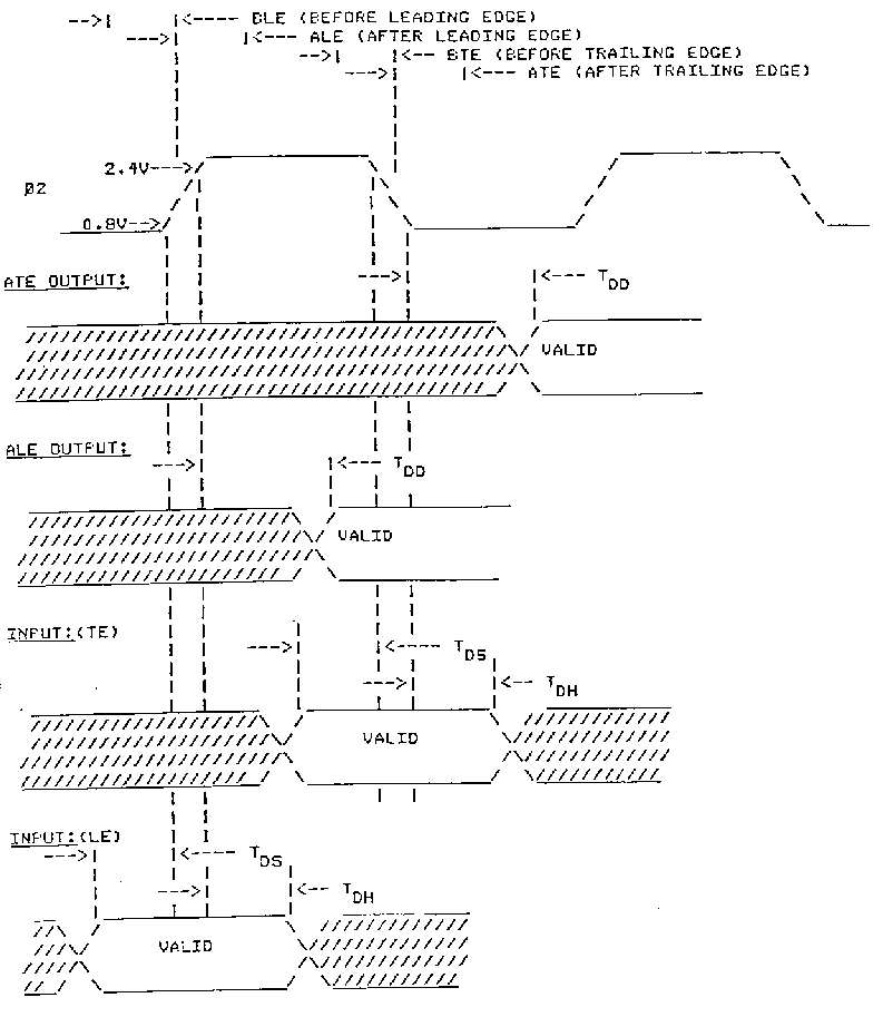
INPUT TIMING
(VDC = 5V ± 5% TA = 0ºC to 70ºC)
| Parameter | Note | Signal type | Symbol | Min | Max | Unit | |
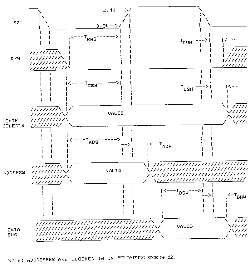
| R/!W setup time | BLE Ø2 | TRWS | 130 | ns | |||
| R/!W hold time | ATE Ø2 | TRWH | 30 | ||||
| Address setup time | A0-A3, A8-A15 | BLE Ø2 | TADS | 130 | |||
| Address hold time | ALE Ø2 | TADH | 30 | ||||
| Chip Select setup time | BLE | TCSS | 50 | ||||
| Chip Select hold time | ATE | TCSH | 30 | ||||
| Data setup time | D0-D7 | BTE Ø2 | TDSW | 130 | |||
| Data hold time | ATE Ø2 | TDHW | 10 | ||||
| Data setup time | |KR1, !KR2, P0-7, SID, BCLK | BTE Ø2 | TDS | 150 | |||
OUTPUT TIMING
(VDC = 5V ± 5% TA = 0ºC to 70ºC)
| Parameter | Note | Signal type | Symbol | Min | Max | Unit | |
| Data setup time | D0-D7 | 2 | BTE | TDSR | 50 | ns | |
| Data hold time | ATE | TDHR | 20 | ||||
| Data delay time | !IRQ | 1 | ATE | TDD | 350 | ||
| Data delay time | SOD, BCLK, OCLK | 1 | ATE | TDD | 350 | ||
| Data delay time | AUD | 3 | ATE | TDD | 200 | ||
| Data delay time | !K0-5 | 1 | ATE | TDD | 1500 | ||
| Data delay time | P-07 | 1 | ALE | TDD | 1500 | ||
Note:
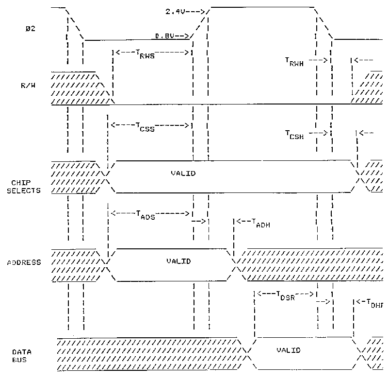
Note: Addresses are clocked in on the rising edge of Ø2.
Note: Addresses are clocked in on the rising edge of Ø2.
| Write | Read | |||
| Register | Name | Description | Name | Description |
| 00 | AUDF1 | Audio Channel Frequency | POT0 | Read the value of each pot |
| 01 | AUDC1 | Audio Channel Control | POT1 | |
| 02 | AUDF2 | Audio Channel Frequency | POT2 | |
| 03 | AUDC2 | Audio Channel Control | POT3 | |
| 04 | AUDF3 | Audio Channel Frequency | POT4 | |
| 05 | AUDC3 | Audio Channel Control | POT5 | |
| 06 | AUDF4 | Audio Channel Frequency | POT6 | |
| 07 | AUDC4 | Audio Channel Control | POT7 | |
| 08 | AUDCTL | Audio Channel Control | ALLPOT | Read 8-line pot port state |
| 09 | STIMER | Character base address | KBCODE | Keyboard code |
| 0A | SKRES | Wait for horizontal blank synchronization | RANDOM | Random Number Generator |
| 0B | POTGO | Wait for horizontal blank synchronization | ||
| 0C | ||||
| 0D | SEROUT | Serial port output register | SERIN | Serial port input register |
| 0E | IRQEN | Maskable interrupt (IRQ) enable | IRQSTAT | IRQ Interrupt status register |
| 0F | SKCTLS | Serial port 4 key control | NMIST | NMI status |
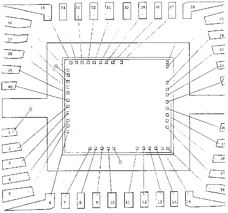
| Vss | 1 | -POKEY- | 40 | d2 | <-> | |
| <-> | d3 | 2 | 39 | d1 | <-> | |
| <-> | d4 | 3 | 38 | d0 | <-> | |
| <-> | d5 | 4 | 37 | aud | --> | |
| <-> | d6 | 5 | 36 | a0 | <-- | |
| <-> | d7 | 6 | 35 | a1 | <-- | |
| --> | Ø2 | 7 | 34 | a2 | <-- | |
| --> | p6 | 8 | 33 | a3 | <-- | |
| --> | p7 | 9 | 32 | r/!w | <-- | |
| --> | p4 | 10 | 31 | !cs1 | <-- | |
| --> | p5 | 11 | 30 | cs0 | <-- | |
| --> | p2 | 12 | 29 | !irq | --> | |
| --> | p3 | 13 | 28 | sod | --> | |
| --> | p0 | 14 | 27 | oclk | --> | |
| --> | p1 | 15 | 26 | bclk | <-> | |
| --> | !ks2 | 16 | 25 | !ks1 | <-- | |
| Vdd | 17 | 24 | sio | <-- | ||
| <-- | !k5 | 18 | 23 | !k0 | --> | |
| <-- | !k4 | 19 | 22 | !k1 | --> | |
| <-- | !k3 | 20 | 21 | !k2 | --> |
| Scale: | 20:1 |
| Package: | 2004,000-3 |
| Wire Bond: | 1.1 mil gold T.C. |
| Die Size: | 179 x 159 mils |
| Die Attach Cavity: | 210 x 230 |
| Comment | Six micron design rules |
<six pages of very hard-to-read circuit diagrams. Some bits are unreadable>